![]()
MIT engineers build advanced microprocessors from carbon nanotubes.
The new approach uses the same manufacturing processes as silicon chips and provides significant advances in the development of next generation computers.
After years of addressing many development and manufacturing challenges, MIT scientists have developed a state-of-the-art microprocessor based on carbon nanotube transistors, which is widely regarded as a faster, greener alternative to their traditional silicon counterparts.
The microprocessor, described today in the journal Nature, can be fabricated using conventional silicon chip fabrication techniques and represents an important step towards more practical application of carbon nanotube microprocessors.
Silicon transistors - critical microprocessor components that switch between 1 and 0 bits to perform calculations - have been established in the computer industry for decades. As predicted by Moore's Law, every few years the industry has been able to downsize transistors and place more chips in place to do increasingly complex calculations. But experts are predicting a time when silicon transistors will no longer shrink and become more and more ineffective.
The fabrication of carbon nanotube field effect transistors (CNFETs) has become an important goal in the construction of next-generation computers. Research shows that CNFETs have properties that promise about 10-fold energy efficiency and much higher speeds compared to silicon. But if the transistors are made on a small scale, they often have many shortcomings that affect performance, so they are not practical.
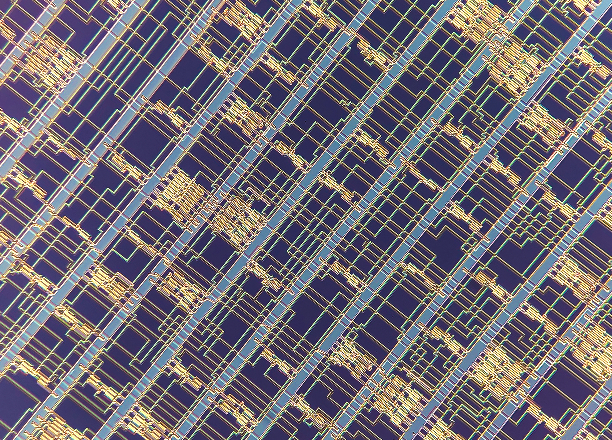
A close-up of a modern microprocessor made up of carbon nanotube field effect transistors. Acknowledgments - Image: Felice Frankel, MIT
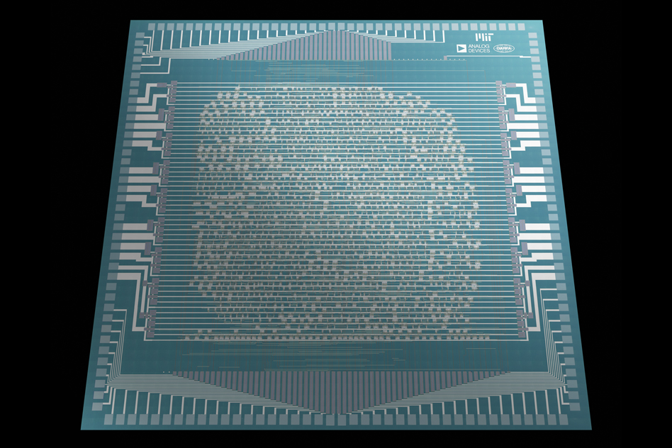
MIT researchers have developed new techniques to drastically reduce defects and allow complete control over the function of manufacturing CNFETs using processes in traditional silicon chip foundries. They demonstrated an 16-bit microprocessor with more than 14.000 CNFETs, which performs the same tasks as commercial microprocessors. The Nature Paper describes the design of the microprocessor and includes more than 70 pages describing the manufacturing method.
The microprocessor is based on the open source chip architecture RISC-V, which contains a series of instructions that a microprocessor can execute. The researchers' microprocessor was able to precisely execute the entire instruction set. A modified version of the classic "Hello, World!" Program that was printed out, "Hello, World!" I'm RV16XNano, made from CNTs. "
"This is by far the most advanced chip from a fledgling nanotechnology that holds great promise for high-performance, energy-efficient computing," says co-author Max M. Shulaker, the Emanuel E Landsman Career Development Assistant Professor of Electrical Engineering and Computer Science (EECS) and Member of Microsystems Technology Laboratories. “There are limits to silicon. If we are to continue making advances in computing, carbon nanotubes are one of the most promising ways to push these limits.
Along with Shulaker, the following people work on the project: first author and postdoc Gage Hills, graduate students Christian Lau, Andrew Wright, Mindy D. Bishop, Tathagata Srimani, Pritpal Kanhaiya, Rebecca Ho, and Aya Amer, all from EECS; Arvind, Johnson Professor of Computer Science and Engineering and Researcher in the Laboratory of Informatics and Artificial Intelligence; Anantha Chandrakasan, Dean of Engineering School and Vannevar Bush Professor of Electrical Engineering and Computer Science; and Samuel Fuller, Yosi Stein and Denis Murphy, all analog devices.
The MIT engineers have built a modern microprocessor from carbon nanotube field effect transistors (in the picture), which are considered to be faster and more environmentally friendly than silicon transistors. The new approach uses the same manufacturing processes as for silicon chips. Acknowledgments - Image: Felice Frankel, MIT
Combating the "curse" of CNFETs
The microprocessor builds on an earlier simulation developed by Shulaker and other researchers six years ago that had only 178 CNFETs and ran on a single bit of data. Since then, Shulaker and his MIT colleagues have tackled three specific issues in device manufacturing: material defects, manufacturing defects, and functional issues. Hills took over most of the microprocessor design, while Lau took over most of the manufacturing.
For years, the flaw inherent in carbon nanotubes has been a “curse of the field,” says Shulaker. Ideally, CNFETs need semiconducting properties to turn their conductivity on and off according to bits 1 and 0, but inevitably a small portion of the carbon nanotubes will be metallic and will slow down or stop the transistor. In order to be resistant to these failures, modern circuits require carbon nanotubes with a purity of about 99,999999 percent, which is practically impossible to manufacture today.
The researchers developed a technique called DREAM (acronym for “Design Resiliency against Metallic CNTs”) that positions metallic CNFETs so that they do not interfere with data processing. In doing so, they relaxed these strict purity requirements by about four orders of magnitude - or 10.000 times - which means that they only need carbon nanotubes with a purity of about 99,99 percent, which is currently possible.
Designing circuits basically requires a variety of different logic gates connected to transistors that can be combined to create adders and multipliers, for example - like combining letters in the alphabet to create words. The researchers found that the metallic carbon nanotubes affect different pairings of these gates differently. For example, a single metallic carbon nanotube in gate A can break the connection between A and B. However, multiple metallic carbon nanotubes in Gate B cannot interfere with any of their connections.
In chip design, there are many ways to implement code on a circuit. The researchers performed simulations to find all the different gate combinations that are tough and resistant to metallic carbon nanotubes. They then adapted a chip design program to automatically determine the combinations that are least affected by metallic carbon nanotubes. When designing a new chip, the program uses only the robust combinations and ignores the vulnerable combinations.
"The play on words 'dreaming' is entirely intentional because it is the dream solution," says Shulaker. "This enables us to buy carbon nanotubes off the shelf, toss them onto a wafer and simply set up our circuit as usual without doing anything else."
Exfoliation and tuning
CNFET production begins with the application of carbon nanotubes in a solution to a wafer with prefabricated transistor architectures. However, some carbon nanotubes inevitably stick together randomly to form large stacks - like strands of spaghetti shaped into small spheres - that create a large particle contamination on the chip.
To eliminate this contamination, the researchers created RINSE (for "Removing Incubated Nanotubes by Selective Exfoliation"). The wafer is pretreated with a preparation that promotes the adhesion of carbon nanotubes. The wafer is then coated with a specific polymer and immersed in a special solvent. This washes away the polymer, which only carries away the large bundles while the individual carbon nanotubes stick to the wafer. The technique leads to an approximately 250-fold reduction in the particle density on the chip compared to similar methods.
Finally, the researchers looked at common functional problems with CNFETs. Two types of transistors are required for binary computing: "N" types, which switch on with a 1 bit and off with a 0 bit, and "P" types, which have the opposite effect. Traditionally, it was difficult to manufacture the two types from carbon nanotubes, which often resulted in transistors with different performance levels. For this solution, the researchers developed a technique called MIXED (for “Metal Interface Engineering crossed with electrostatic doping”), which precisely adjusts transistors for function and optimization.
In this technique, they bind certain metals to each transistor - platinum or titanium - which allows them to fix that transistor as P or N. They then coat the CNFETs in an oxide compound by atomic layer deposition, which enables them to tune the properties of the transistors for specific applications. For example, servers often need transistors that work very quickly, but at the same time carry energy and performance. Wearables and medical implants, on the other hand, can use slower, low-power transistors.
The main goal is to get the chips into the real world. To this end, the researchers have now started to implement their manufacturing techniques in a silicon chip foundry through a program of the Defense Advanced Research Projects Agency, which supports the research. While no one can say when chips made entirely from carbon nanotubes will hit shelves, Shulaker says it could be less than five years. “We think it's no longer about if, but when,” he says.
The work was also supported by Analog Devices, the National Science Foundation and the Air Force Research Laboratory.
Article: MIT / ISE, image: Felice Frankel, MIT